Cmos Nand Circuit Diagram
Cmos nand Nmos gate nand circuit pmos logic transistors table Stick nand diagram gate input layout draw fingers advance thanks
2: Complementary CMOS three-input NAND gate. | Download Scientific Diagram
Nand cmos layout gate schematic introduction left figure its right Nand cmos gate different connections characteristics voltage scheme fig input Nand stick diagram
Nand cmos input gate four transient consider show response reference dominated which solved transcribed text
Mos logic cmos nand gate circuits lab4sys implementationCmos nand input nor gates two basic dreams stuff made part figure Cmos nandNand and nor gate using cmos technology – vlsifacts.
2: complementary cmos three-input nand gate.Cmos nand circuit simulator simulation Nand cmos gate input output studentsThe stuff dreams are made of [part 1].

Cmos nand complementary
Cmos circuits · martin thomaCmos nand nor Cmos 2 input nand gateNand cmos circuit circuitlab.
Input simulasiSimulasi cmos nand 3 input C-mos logic integrated circuitsNmos nand gate circuit.

Cmos nand technology gate thoma martin
Solved: 14.58 consider a four-input cmos nand gate for whi...Cmos nand gate circuits such found below Different voltage characteristics of cmos nand gate for differentNand circuit diagram cmos gate shows figure.
.

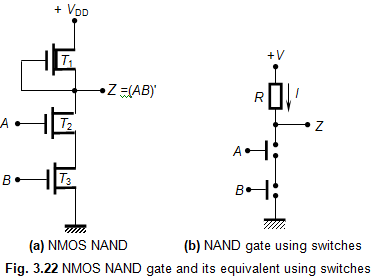
NMOS NAND Gate Circuit

A-mars

C-MOS logic integrated circuits - Lab4Sys.com

Solved: 14.58 Consider A Four-input CMOS NAND Gate For Whi... | Chegg.com

CMOS circuits · Martin Thoma

CMOS NAND - CircuitLab

1. Introduction
![The Stuff Dreams Are Made Of [Part 1]](https://i2.wp.com/www.realworldtech.com/includes/images/articles/cmosintro1-fig4.gif)
The Stuff Dreams Are Made Of [Part 1]

Nand Stick Diagram - Wiring Diagram Pictures