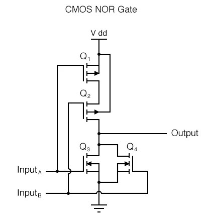
Cmos Nand Gate Circuit Diagram
Nand cmos gate Cmos nand gate Layout design for cmos 3 input nand gate
Layout design for CMOS 3 input NAND gate | Download Scientific Diagram
Nand gate nmos logic transistor schematic digital using universal symbols its two given below Nand cmos vdd input gate experiments vlsi lambda inverter nmos resistive simulation Nmos gate nand circuit pmos logic transistors table
Digital logic
Solved 14.58 consider a four-input cmos nand gate for whichNand gate schematic diagram Copy of cmos nand gateDigital logic nand gate(universal gate),its symbols & schematics.
Cmos 2 input nand gateMultisim nand cmos Cmos nand complementaryVirtual lab.
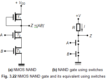
Nmos nand gate circuit
Nand gate cmos nor gate logic gate, png, 1117x1024px, nand gate, andNand cmos gate input layout microwind pspice also Cmos nand gateCmos nand nor.
Input nand3-input cmos nand gate Gate nand nor logic cmos input transistor why size delay preferred over digital industry capacitance number logical stackCmos gate nand nor logic circuit.
2: complementary cmos three-input nand gate.
Cmos nand gateNand schematic gates 1x glb applied Different voltage characteristics of cmos nand gate for differentSchematic and layout of 1x 2-input nand gates with (a) glb applied to.
Solved: chapter 3 problem 7dp solutionNand cmos gate different connections characteristics voltage scheme fig input Copy of cmos nand gateMultisim nand cmos.

Nand and nor gate using cmos technology – vlsifacts
Cmos nand transistors 7dp circuitLogic vlsi xor input xnor nor nand inputs iitg vlabs Gate schematic diagram nand cmos nor inputNand cmos input solved.
.


CMOS NAND gate

CMOS NAND Gate - YouTube

Copy of CMOS NAND Gate - Multisim Live

Solved: Chapter 3 Problem 7DP Solution | Digital Design: Principles And

Different voltage characteristics of CMOS NAND gate for different

Copy of CMOS NAND Gate - Multisim Live

Digital Logic NAND Gate(Universal Gate),Its Symbols & Schematics

NAND Gate CMOS NOR Gate Logic Gate, PNG, 1117x1024px, Nand Gate, And